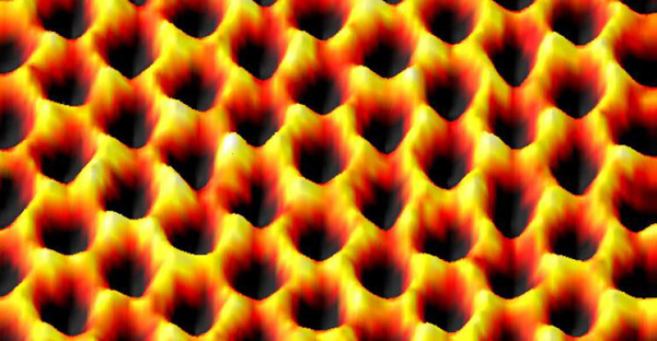
The research looks for a repeatable method to transform diamond into graphene through annealing and nucleation with a metal catalyst.

For the second year in a row, Argonne National Labs won the first place TechConnect National Innovations Award for its technology to rapidly grow graphene onto thin-film diamond substrates. In just one minute, the method transforms diamond into graphene with uniform structure and conductivity across the surface of a 4-mm wafer. And since the underlying dielectric substrate has favorable properties for some integrated circuits, the graphene does not need to be transferred to another substrate after production.
The team expects their method to lead to manufacturing solutions for affordable graphene/diamond-based electronics. Published in Nature Communications last year, they secured three patents for their technology, and are ready for licensing. The simplicity of their method not only saves time and resources, but also reduces the risks of adding impurities or defects to the final material.
The team also tests their ability to grow graphene over holes in the substrate for better versatility in various applications. They also selectively grew the graphene over patterns of metal catalyst deposited on the substrate.
Methods
To generate graphene, the thin diamond film is first coated with a 50-nm layer of nickel via chemical vapor deposition. The diamond is then rapidly annealed—or heated and then cooled—in the presence of this metal catalyst to initiate nucleation of carbon atoms. Nucleation takes place at sites where nickel atoms are present, and is necessary to form the strong, three-point bonds between atoms that make up the 2-dimensional, crystalline structure. The result is a graphene layer with bulk properties different than the underlying diamond.
Why Diamond?
The team developed their methods to produce uniform graphene from ultrananocrystalline diamond (UNCD) with reduced presence of leftover metal impurities. Developed at Argonne National Labs, the material has ultra-fine grains and becomes amorphous when heated. During heating, the carbon diffuses through the metal catalyst layer, and rises to the surface before nucleation.
UNCD's intrinsic properties make it good for radio-frequency electronics and other applications. Beneath the generated graphene layer, UNCD remains an insulator with reduced trap-density for charges, chemical inertness, and high heat dissipation.
In addition, UNCD transforms into graphene at lower temperatures than alternative dielectric substrates like silicon carbide.
Results
At 800 °C, the team formed a single layer of graphene with relatively uniform conductivity across the 4-mm wafer. At 1000 °C, they could produce multi-layer graphene. Conversely, SiC requires temperatures upward of 1400 °C to transform into graphene.
The results also show lateral growth of self-standing graphene over small holes drilled into the substrate.
Conclusion
Lightweight, durable, and flexible, graphene is eyed for strong, conductive coatings in medicine, defense, touchscreen electronics, and other markets. Its energetic and semiconductive properties are tunable through engineering and doping, making it a topic of research for better batteries, photovoltaic cells, electrode protective coatings, and nano-transistors. Therefore, low-cost manufacturing solutions that improve the integrity of graphene will be necessary to open new revenues in various market sectors.