
This article introduces the wide application range of silicon carbide and its new expansion in the application fields.
As is known to all, silicon and germanium constitutes the first generation of semiconductor materials, which is mainly used in low pressure, low frequency, the power transistor and photoelectric detector. Compared with germanium semiconductor devices, semiconductor devices made of silicon materials have good high temperature resistance and radiation resistance.
More than 95% of semiconductors and 99% of integrated circuit are made of silicon semiconductor materials. Until now, we are using semiconductor products that are mostly based on silicon materials. After 1990s, gallium arsenide and indium phosphide represent the second generation of semiconductor materials that can be used for making high speed, high frequency, high power and light electronic devices.
With the rise of information superhighway and Internet, the second generation of semiconductor materials are widely used in satellite communication, mobile communication, optical communication and GPS navigation and other fields.
Compared with the first two generation of semiconductor materials, the third generation of semiconductor material is usually referred to as wide-band gap semiconductor material or high temperature semiconductor material. Among them, silicon carbide and gallium nitride are the representatives with mature development in the third generation of semiconductor materials. In the development of wide-band gap semiconductors, silicon carbide (SiC) semiconductor material is the most mature research achievement.
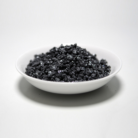
Silicon carbide semiconductor materials with wide band gap, high breakdown electric field, high heat conductivity, high saturated electron mobility as well as the characteristics of smaller volume, has great potential at high temperature, high frequency, high power, optoelectronics and the application of radiation device.
The application range of silicon carbide is very wide:
A. Because of the characteristics of wide-band gap, it can be used to make blue light-emitting diodes or the ultraviolet detector that is almost not influenced by sunlight;
B. Due to the available voltage or electric field being eight times than that of silicon or gallium arsenide, it is especially suitable for manufacturing high voltage power devices such as high voltage diode, power triode, SCR and high power microwave device;
C. Because of the high saturated electron transfer rate, it can be made into all kinds of high frequency components (radio frequency and microwave);
D. Silicon carbide is a good conductor of heat whose thermal conductivity properties is superior to any other semiconductor materials, which makes silicon carbide devices can work properly under high temperature.
E. In addition, silicon carbide has strong ionic covalent bond that has high hardness, higher thermal conductivity than that of copper, good cooling performance, strong corrosion resistance, strong ability to resist radiation, high temperature resistant and good chemical stability, etc, which has been widely used in the field of space technology.
The application of silicon carbide:
At present, the technology that silicon carbide is applied to power transistor and SCR has been basically mature. Using the power circuit made by silicon carbide has small size, high temperature resistant, long service life and other advantages.
For example, in the use of inverter in electric cars, silicon carbide replaces traditional materials, which can shrink nearly 50% of the volume and weight and also greatly extend its service life. As the popularity of solar power station, electric vehicles, and new energy projects such as electric locomotive, the future market of high-power inverter, inverter and machine governor made by silicon carbide will boom rapidly.
Silicon carbide is also a kind of high performance LED (light-emitting diode) substrate material. By using gallium nitride, it can make high brightness LED light that is 3~4 times luminous efficiency and 10 times life expectancy of energy-saving lamps. Because of the small lattice mismatch of silicon carbide and gallium nitride, silicon carbide single crystal is the ideal substrate materials of gan-based LED, schottky diode, metal-oxide-semiconductor field-effect transistor and other devices.
Although the most ideal substrate is gallium nitride single crystal material, it is very hard to make it. Until now, there is no effective way that can do that. Our experts use the silicon carbide single crystal substrate as the breakthrough and have achieved remarkable achievements. Now, the annual output of 70000 pieces of silicon carbide wafer production line has formed, promoting the sustained and stable development of the third generation of semiconductor industry in China, and has achieved good economic benefit and social benefit, which breaks the monopoly of Cree companies in the United States for silicon carbide substrate in the international market.
The current applications of silicon carbide in the electronics industry are mainly based on three major areas: high brightness LED, high-power power electronic system, as well as advanced radar. It may also enter the domestic market in the future. Although solar silicon wafer cutting is unlikely to rise again, as a new type of electronic material, silicon carbide materials’ another spring is just around the corner as long as it is based on science and technology innovation of silicon carbide industry.
Abrasives Suppliers Directory -
Abrasives Buyers Directory -
Abrasives Manufacturers -
Abrasives Online Marketing
Sitemap -
User Agreement -
Terms of Use -
Privacy Policy


