
Semiconductors are integral to modern electronics. Recently, scientists have demonstrated the ability to design and fabricate flexible, high-performance semiconductors out of colloidal nanocrystals.
Semiconductors are integral to modern electronics. Currently, they're made by etching features into silicon, but researchers are constantly exploring new fabrication approaches that balance cost, energy efficiency, electronic capabilities, and mechanical properties.
Recently, scientists have demonstrated the ability to design and fabricate flexible, high-performance semiconductors out of colloidal nanocrystals. The approach allowed them to lay out the circuitry using simple solution processing, in which the components are put in place while suspended in a liquid. Solution processing is generally cheap and convenient, and it can be used to cover large areas at once.
Why nanocrystals?
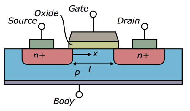
To obtain the right mix of electronic properties, the scientists selected dispersions of silver nanocrystals, aluminum oxide nanocrystals, and cadmium selenide nanocrystals. These were used to create the gate electrode, gate insulator, and semiconducting channel layers, respectively.
Colloidal, inorganic nanocrystals have already been evaluated for use in electronic devices. Previous studies demonstrated that these nanocrystals work well and can be put in place using solution processing. For example, scientists developed nanocrystal inks that exhibit metallic, semi-conducting, and insulating properties. It's also possible to vary their electrical properties based on their individual size, shape, composition, and subsequent assembly.
Device fabrication
In an investigation published in Science, a team of scientists described how they overcame these challenges through a series of solution-based processing steps. Their nanocrystal device was fabricated on a flexible polymer substrate. First, the bottom gate electrodes were defined. After a pattern was laid out on the polymer surface, a layer of silver nanocrystals was applied via spin coating. Next, the silver coating was chemically treated to enable stacking of the nanocrystal device layers . The pattern was then removed, leaving behind the silver nanocrystal gate electrodes (80 ± 10 nm thickness)
The next component of the device they needed to add was the gate insulator layer. The scientists first treated the substrate with charged polymers to alter the surface charge. Next, the gate insulator was grown in a layer-by-layer fashion with alternating layers of aluminum oxide nanocrystals and poly(styrenesulfonate), each with opposite charges. The final thickness of the gate insulator was 60 ± 5 nm.
Finally, the device was thermally treated for 10 minutes at 250°C in a nitrogen atmosphere. This step made the cadmium selenide film denser. This process was also critical for getting the indium to diffuse into the source and drain electrodes.
Device characterization
The scientists tested out the performance of the resulting devices. They found that the silver nanocrystal films were uniform and crack-free, and they had a small amount of surface roughness. These films produced well-defined electrodes. Additionally, the aluminum oxide insulator layers were continuous and smooth.
The researchers found that the dielectric constant of the aluminum oxide nanocrystal insulator layer was 15.1 at 50Hz using capacitance voltage measurements. This dielectric constant is higher than that of the typical aluminum oxide layers due to the presence of the polymer, which allows more efficient charge accumulation at low voltages. After heat treatment, the aluminum oxide nanocrystal layer also exhibited low current leakage densities of 7.16 x 10⁻⁷ A/cm2 and ~2.2 x 10⁻⁷ A/cm2 at an applied electric field of 300 kV/cm. The electrical performance of such a thin aluminum oxide gate was critical for the development of low-voltage and high-performance flexible nanocrystal electrodes.
The integrated device operated at low voltages and exhibited characteristics of a typical n-type field-effect transistor. The demonstration that solution processing can make a competitive device suggests a new route for the development of large-area, low cost, and flexible electronics. This could open up the possibility for new processing methods, including the development of such devices via 3D printing.
Abrasives Suppliers Directory -
Abrasives Buyers Directory -
Abrasives Manufacturers -
Abrasives Online Marketing
Sitemap -
User Agreement -
Terms of Use -
Privacy Policy


