
Edmund Optics® (EO), the premier provider of optical components, introduces new Fused Silica Wafers. These versatile wafers are thin, circular pieces of UV fused silica designed to be used as test substrates to measure the quality of optical coatings.
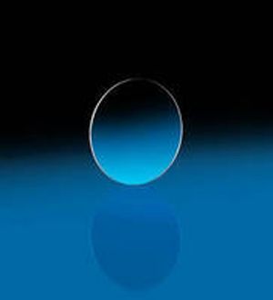
Exhibiting less than 10 Å surface roughness with surface quality of 40-20, TECHSPEC® Fused Silica Wafers are thin, circular pieces of UV fused silica designed to be used as test substrates to measure quality of optical coatings. Each is ultrasonically cleaned and delivered in contaminant-free packaging. Available in 100, 200, and 300 mm diameters, RoHS-compliant wafers have thickness of 1.00 mm and transmission range of 0.2–2.2 µm。
Edmund Optics® (EO), the premier provider of optical components, introduces new TECHSPEC® Fused Silica Wafers. These versatile wafers are thin, circular pieces of UV fused silica designed to be used as test substrates to measure the quality of optical coatings. Fused Silica Wafers are also outstanding for use as dummy components for set-up processes, as well as for semiconductor microlithography or for micro-electronic-optical applications (MEMS).
Ultrasonically cleaned
Edmund Optics' Fused Silica Wafers Exhibit less than 10Å Surface Roughness with a surface quality of 40-20. Each Fused Silica Wafer has been ultrasonically cleaned and is delivered in contaminant-free packaging to ensure highest quality.
Available in 100 mm, 200 mm and 300 mm diameters
Edmund Optics' Fused Silica Wafers are available in 100 mm, 200 mm and 300 mm diameter sizes. RoHS compliant, all have thicknesses of 1.00 mm and a transmission range of 0.2-2.2 μm. Fused Silica Wafers are in-stock and available for immediate delivery for fast turnaround and excellent value.
See more at: http://www.iabrasive.com/.
Abrasives Suppliers Directory -
Abrasives Buyers Directory -
Abrasives Manufacturers -
Abrasives Online Marketing
Sitemap -
User Agreement -
Terms of Use -
Privacy Policy


