
Recently, another product made in China is available! That is the high purity semi-insulating silicon carbide substrate of four and a half inches.
Recently, another product made in China is available! That is the high purity semi-insulating silicon carbide substrate of four and a half inches. Experts of China's Electronic Material Industry Association believe that the achievement is in the domestic leading position and has reached the international advanced level. Before that, a company in Beijing has successfully developed silicon carbide substrate from 2 inches to 6 inches with the Chinese Academy of Sciences, completing the process of silicon carbide semiconductor from scratch in our country. Today, our second enterprise also realizes the large-scale production of silicon carbide materials, which marks the development of silicon carbide materials gradually heading into mature in our country.
Tech-watchers learns about this is a silicon carbide production enterprise. Materials science and technology has been one of short boards of China's military development. In January, 2015, Tech-watchers reported that a company in Beijing cooperated with the Chinese Academy of Sciences and successfully developed silicon carbide substrate of 6 inches, and formed a silicon carbide wafer production line whose annual output can reach 70000 pieces. Once the enterprise is the only silicon carbide semiconductor materials production enterprise in China. However, the short board of materials science and technology is not only reflected in technology, but also on the production. Although there is a gap compared with the technology, but Tech-watchers understands that new production line of the second company will reach the annual output of 40-500000 silicon carbide substrate of four inches. Such a huge scale is likely to mean that the reduction of the cost of silicon carbide products in our country and the leap in production.
At present, as is known to all that most of semiconductor materials are monocrystalline silicon, and our monocrystalline silicon has mainly relied on imports for a long time. Compared with monocrystalline silicon, the production and application of silicon carbide materials have been very difficult. The current countries that research and develop silicon carbide devices in the world are mainly the United States, Germany, Switzerland, Japan and other countries, but until now the industrial application of silicon carbide is mainly used as abrasive (BRDF). Swiss ABB once successfully developed the sic diodes, but in 2002, ABB terminated the project about silicon carbide because of technological difficulties and some uncertainty, which can show visible development difficulties.
The important strategic value of semiconductor silicon carbide substrate and chips is to make it always rank in the U.S. department of commerce embargo list, which also causes our country difficult to obtain corresponding products from abroad. The enterprise in our country has successfully developed high purity semi-insulating silicon carbide substrate of four and a half inches, which shows we have been able to get rid of dependence on abroad in the silicon carbide wafer products on the process and production, heading into the self-determination mass production and widespread application.
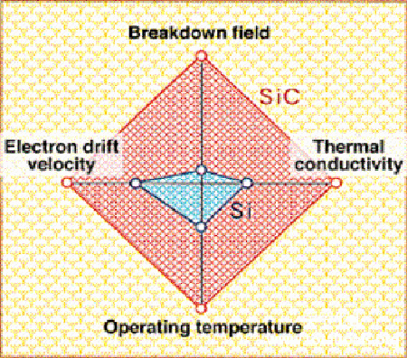
The physical property of silicon carbide is quite different from that of silicon. Monocrystalline silicon carbide has more excellent physical properties compared with monocrystalline silicon, such as about 10 times the electric field intensity, about three times higher thermal conductivity, about 3 times the width of the forbidden band, about twice as high saturation drift velocity. In addition, on the specific application, although the technology difficulty of silicon carbide devices is larger than monocrystalline silicon, but once the problem of process is solved, the manufacturing process of silicon carbide devices is short, with small volume and weight, the oxidation resistance, long life, high output power, etc. These characteristics will make it far better than that of monocrystalline silicon and become the ideal semiconductor materials in the 21st century. What’s more, the energy consumption of silicon carbide materials is extremely low. If the annual output is of 400000 pieces of silicon carbide wafer substrate, applied only in the field of lighting, it will reduce the consumption of electricity every year that is equivalent to save 26 million tons of standard coal. It is really an ideal energy-saving materials.
With the rapid development of wireless communication technology, the demand for hardware system high power density and the response speed is becoming increasingly urgent. The transistor based on silicon carbide materials has incomparable advantages over monocrystalline silicon and gallium arsenide devices in the field of microwave radio frequency, which is suitable for aerospace, microwave communication, electronic countermeasures, large capacity information processing and other applications. Along with the increasing ability of the silicon carbide wafer production, domestic aircraft, warships will be able to be changed into new and better "clairvoyance", narrowing the gap and the United States on the quality and quantity to. In addition, civil semiconductor and power field are also in urgent need for silicon carbide materials.
Abrasives Suppliers Directory -
Abrasives Buyers Directory -
Abrasives Manufacturers -
Abrasives Online Marketing
Sitemap -
User Agreement -
Terms of Use -
Privacy Policy


