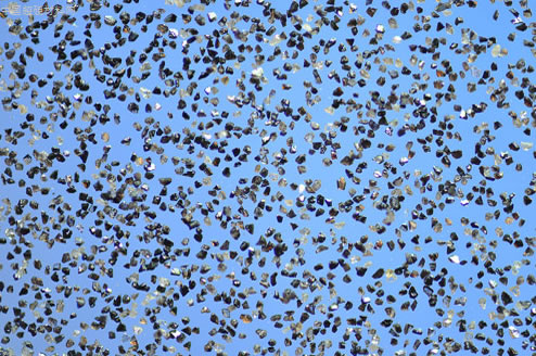
Jay Narayan from North Carolina State University develops a kind of new preparation method about hexagonal boron nitride into cubic boron nitride with his team,whose conversion speed and preparation cost are faster and cheaper than traditional process.

Jay Narayan, a professor from North Carolina State University (NCSU), developed a kind of new preparation method about hexagonal boron nitride (h - BN) into cubic boron nitride (CBN) with his team, whose conversion speed and preparation cost are faster and cheaper than traditional process. It is expected to be used in high power electronic devices, transistors, solid state components and other applications.
There are four basic forms about boron nitride, and h-BN and CBN of them are the two kinds that are most widely used in electronic equipment field, whose structure and properties are similar to diamond and graphite. On integrated circuit applications, CBN has great thermal conductivity performance, whose high frequency power performance can be comparable to silicon phase.
This new preparation method of NCSU team can not only produce traditional cubic boron nitride, but also make a new material called Q-boron nitride (Q-BN). "Q" represents the "quenching" phase of this material, which needs to be heated to a certain temperature and then quickly cooled. As early as 2015, in the Journal of Applied Physics, the team published the study about Q-carbon - a new phase of carbon; The Q-BN development is built on this basis.
Narayan said: "This is another technological achievement after the research and development of Q-carbon and Q-carbon into diamond. With the help of power control and time control, we skirt successfully the thermodynamic technology bottleneck of boron nitride, and develop a new-type phase of boron nitride ".
The study is published in APL materials journal. Narayan and his team use h-BN layer that has better thermal stability and the thickness about 500-500 nm, to produce Q-BN and CBN. Place the h-BN layer on the substrate, and then use high power laser pulse to heat it to 2530 ℃, and the substrate will absorb the heat and complete the “quenching” for h-BN layer. The whole experiment process is carried out at room temperature, which only takes one fifth microseconds.
The key of this experiment is the substrate preparation below h-BN layer, which affects the cooling speed of h-BN layer. Through the control of the cooling process, it can determine that the product is traditional CBN or new Q-BN.
The biggest advantage of new method about h-BN into CBN is its low cost. It can be operated under room temperature and pressure, whose required temperature is relatively low; And the traditional process needs to raise the temperature to 3225 ℃ and pressure up to 95000 atmospheres.
Low and rapid preparation technology makes CBN more conveniently applied in study of applications of electronic equipment, whose advantages are more than diamond. For example, the band gap of CBN is higher than diamond, and it has more advantages in high power devices.
Narayan adds that we now can make use of CBN to produce large area of single crystal film, and also make n & p type dopant plating, used for research and development of high power transistor and change-over switch. These technologies can replace heavy volume transformer and build the next generation power grid for super electric power highway.