
Researchers in Sweden are building 3D silicon carbide devices on standard silicon wafers as part of a €8m international project
Researchers in Sweden are building 3D silicon carbide devices on standard silicon wafers as part of a €8m international project
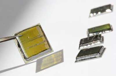
Professor Rositsa Yakimova, Docent Mikael Syväjärvi and the research group at the Semiconductor Materials Division of Linkõping University were among the first to manufacture wafers of high-quality cubic silicon carbide. Together with 13 partners from six European countries and Japan, they are now developing tools to make it possible to manufacture cubic silicon carbide on a substrate of silicon, without large numbers of crystal defects arising.
The four year Horizon 2020 programme Challenge brings together leading European researchers in silicon carbide and small and large companies. The four-year project is led by Francesco La Via, of the Italian Consiglio Nazionale delle Ricerche and includes Novasic in France, Anvil Semiconductors and the University of Warwick in the UK, Ascatron in Sweden and chip maker STMicroelectronics. Silvaco Europe is providing design tools.
The aim of the project is to develop functional semiconductor materials for new power components that will make the motors used in electric cars more efficient, with lower heat loss. At voltages above 1200 V, electronic components using hexagonal silicon carbide, 4H-SiC, are now commercially available but expensive. The consumer market is highly price-sensitive, and it is here that cubic silicon carbide, 3C-SiC, comes in.
3C-SiC is most efficient at voltages between 600 and 1200V and the aim is to build these devices on large siliocn wafers for cost effective manufacturing by overcoming defects in the interface between the cubic silicon carbide and the silicon substrate.
“After many years’ research, we have developed a method to produce cubic silicon carbide with few defects, and our material is to be used as reference. In the project centred on power electronics, the cubic silicon carbide must be grown on, for example, silicon, but we believe that developments will lead to other applications in which the quality of our material gives advantages,” said Syväjärvi at Linkõping.
Abrasives Suppliers Directory -
Abrasives Buyers Directory -
Abrasives Manufacturers -
Abrasives Online Marketing
Sitemap -
User Agreement -
Terms of Use -
Privacy Policy


